PCB Trace Impedance Calculator
Use this PCB Impedance Calculator to determine the characteristic impedance (Z₀) of PCB traces. Enter the Trace Width (W), Substrate Height (H), Dielectric Constant (er), and Copper Thickness (T) to calculate PCB Trace Impedance (Z₀) for accurate signal integrity, controlled impedance design, and high-speed PCB applications.
Enter the values of Trace Width (W), Substrate Height (H), Dielectric Constant (er), and Copper Thickness (T) to calculate the PCB Trace Impedance (Z₀).
Result
PCB Trace Impedance (Z₀)
Ohm
What is PCB Trace Impedance?
PCB Trace Impedance (Z₀) is the characteristic impedance of a PCB trace. It determines how electrical signals propagate along the trace and is critical for maintaining signal integrity in high-speed circuits. Impedance depends on the trace geometry, substrate material, copper thickness, and dielectric constant of the PCB.
Uses of PCB Trace Impedance in PCB Design
- Ensures signals are transmitted without reflection or distortion.
- Critical for high-speed digital circuits, RF circuits, and controlled impedance designs.
- Helps in matching impedance with components, connectors, or transmission lines.
- Reduces signal integrity issues such as crosstalk, ringing, or overshoot.
Use of PCB Impedance Calculator
This PCB Impedance Calculator helps engineers and designers:
- Quickly calculate the characteristic impedance (Z₀) for single-ended PCB traces.
- Optimize trace width, substrate height, copper thickness, and dielectric material for controlled impedance.
- Avoid costly PCB redesigns by predicting impedance before fabrication.
- Ensure reliable signal performance in high-speed or RF PCB designs.
Equation of PCB Trace Impedance
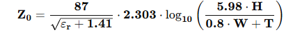
where
Z₀ - PCB Trace Impedance (Z₀) (Ohms (Ω))
W - Trace Width (Mils)
H - Substrate Height (distance from trace to ground plane) (Mils)
T - Copper Thickness (Mils)
εr - Dielectric Constant of PCB material (Dimensionless)
log10 - Base-10 logarithm (Mathematical operation)
Explanation:
H and W determine the geometrical ratio of the microstrip trace.
T (copper thickness) affects the effective width of the trace.
εr adjusts for the PCB substrate material’s dielectric effect on signal propagation.
The constant 87 and the formula structure are derived from IPC-2141B and standard microstrip impedance equations for PCB design.
This formula ensures that your PCB traces have the correct impedance to minimize reflections and maintain signal quality.
Applications of PCB Trace Impedance
- High-speed digital circuits (DDR, PCIe, USB, Ethernet)
- RF and microwave PCBs for wireless devices
- Controlled impedance designs for sensitive analog signals
- Multi-layer PCB design for servers, routers, and telecommunications equipment
- Ensuring reliable signal transmission in automotive and industrial electronics