PCB Trace Width Calculator
PCB Trace Width Calculator can determine the width of a copper trace that can carry a certain amount of current without exceeding the desired temperature rise. Enter the current, temperature of the surrounding environment, the thickness of the copper layer, trace length, and the permissible temperature rise of the trace during current flow. The calculator will then display the trace width and required resistivity of both internal and external copper traces.
Enter the values of current, ambient temoerature, thickness, trace length and temperature rise and then click on calculate to get all the PCB trace width parameters.
What is PCB trace Width?
PCB trace width is the measurement of the conductive copper path on a printed circuit board (PCB) designed to carry an electrical current. This width is crucial for ensuring that the current flow does not exceed the trace’s capacity, which would otherwise cause excessive heating and potential damage to the PCB and its components. Various factors, including the amount of current, copper thickness, ambient temperature, and the goal of the temperature rise, affect the optimum trace width. By following certain standards like IPC-2221, a calculation is made to size up the proper trace width to support the components with electrical current reliably, guaranteeing lasting functionality and lifespan of devices used in different applications.
Inputs:
- Current (I): The current the trace must carry, in Amperes (A).
- Ambient Temperature: The temperature of the surrounding environment, in degrees Celsius (°C).
- Thickness (t): The thickness of the copper layer in ounces per square foot (oz/ft²).
- Trace Length (L): The length of the trace, in meters (m).
- Temperature Rise (T_Rise): The permissible temperature rise of the trace during current flow, in degrees Celsius (°C).
Calculation Formulas:
- Calculate the Area (A): The area of the copper trace required to carry the specified current is calculated using the formula:

Where:
- A = Cross-sectional area of the trace (mm²)
- I = Current (A)
- TRise = Allowed temperature rise (°C)
- k, b, c = Constants based on internal or external trace conditions
2. Calculate the Width (W): After determining the area, the width of the trace can be calculated using:
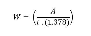
Where:
- W = Width of the trace (mil)
- A = Cross-sectional area (mm²)
- t = Copper thickness (oz/ft²)
- 1.378 is a conversion factor for copper thickness in ounces.
Outputs:
- Trace Width (Internal): This is the width, in mils, of traces needed on the internal layers of the PCB itself.
- Trace Width (External): The width of the trace on outside layers, in mils.
- Resistivity (Copper Internal): Resistance of the copper trace for internal layers, in ohms.
- Resistivity (Copper External): The resistance of the copper trace for external layers, in ohms.