Pad Diameter Calculator
Use this Pad Diameter Calculator to find the correct PCB pad size. Enter the Hole Diameter and Annular Ring to calculate the required Pad Diameter.
Enter Hole Diameter and Annular Ring to calculate the Pad Diameter.
Result
Pad Diameter Calculator
mm
What is Pad Diameter?
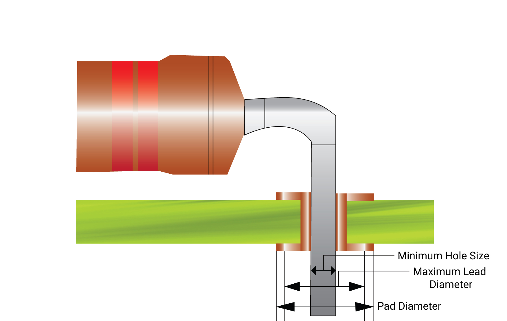
The Pad Diameter is the total diameter of a PCB pad surrounding a drilled or plated hole. It provides mechanical support and reliable soldering for component leads while ensuring proper electrical connectivity.
The pad diameter depends on two main factors:
- Hole Diameter: The size of the drilled or plated hole to accommodate the component lead.
- Annular Ring: The additional copper area around the hole to ensure mechanical strength, solder coverage, and electrical reliability.
By combining these, the pad ensures that components are securely mounted and maintain electrical and mechanical integrity during assembly and operation.
Uses of Pad Diameter Calculation
Calculating the correct pad diameter is important to ensure reliable PCB manufacturing and soldering.
Common uses include:
- Designing through-hole component pads
- Ensuring sufficient annular ring width
- Preventing pad breakout during drilling
- Improving solder joint reliability
- Meeting PCB fabrication design rules
Accurate pad diameter helps maintain mechanical strength and electrical reliability of the PCB.
Pad Diameter Calculation
The pad diameter depends on two main parameters:
- Hole diameter
- Annular ring size
The annular ring represents the copper area surrounding the hole, which provides space for drilling tolerances and ensures that enough copper remains after the drilling process.
To obtain the total pad diameter, the annular ring is added on both sides of the hole.
Pad Diameter Equation:
Pad Diameter (mm)=Hole Diameter (mm) + 2×Annular Ring (mm)
where
- Hole Diameter: Component lead hole size
- Annular Ring: Extra copper around the hole for reliability
Applications of Pad Diameter in PCB Design
- PCB Design: Determines correct pad sizes for through-hole and plated-through components.
- Manufacturing: Ensures proper drill and pad dimensions to avoid defects.
- Electronics Assembly: Provides reliable solder joints and prevents pad lift.
- Mechanical Reliability: Offers extra copper for strong component mounting.
- High-Density PCB Layouts: Optimizes pad size while conserving board space.

